"Nature" and "Science" Week (09.19-09.25) Frontiers of Materials Science

Abstract 1. Control the colloid distribution by modulating the molecular orientation in nematic liquid crystals (Controlofcolloidalplacementbymodulatedmolecularorientationinne...
1. Control the colloidal distribution by modulating the molecular orientation in the nematic liquid crystal
(Control of colloidal placement by modulated molecular orientation in nematic cells)
Through the interaction between particles, the colloid can be self-assembled into a variety of organized superstructures. This is a tremendous advancement in the scientific understanding and application of single-type isomorphic particle self-assembly. Due to the presence of thermal perturbations, forming superstructures where colloidal particles occupy a predetermined location and can remain at these locations remains highly challenging. Peng et al. have proposed a general method for guiding colloidal arrangements using nematic liquid crystals in which nematic liquid crystals are provided with pre-applied spatially differently oriented molecules from a photo-alignment substrate. The colloidal particles in the nematic environment are constrained by the long-range elastic forces determined by the nematic alignment rules. The gradient of orientation changes produces an elastic energy distribution that drives the colloid to a specific location through proper deformation. The example shows that the colloidal spheres fixed on the vertical surface are driven to the maximum unfolded area, while the colloidal spheres fixed on the tangential surface are placed in the curved area. By determining the over-damped power of the colloid, a decisive elastic force can be determined. Controlling colloid self-assembly through patterned molecular orientation provides new opportunities for designing materials and devices. (Science Advances DOI: 10.1126/sciadv.1600932)

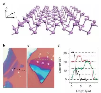
2. Direct observation of the electronic structure in the phosphone
(Direct observation of the layer-dependent electronic structure in phosphorene)
As a monoatomic layer of black phosphorus, phosphonene is a new two-dimensional (2D) material that is expected to be used in electronic and photonic technologies. Li et al.'s experiments show that the electronic structure of multi-layered phosphonene is significantly correlated with its number of layers, which is basically consistent with theoretical predictions. Its inter-band optical transition covers a wide range from visible to mid-infrared, which is important for technical applications. In addition, they observed strong photoluminescence at the energy very close to the absorption edge, indicating that the multilayer phosphonene is a direct bandgap semiconductor. The strong correlation between the number of layers of phosphonene and the electronic structure, combined with its high electron mobility, makes it a more significant advantage in electronic and optoelectronic applications than other two-dimensional materials. (Nature Nanotechnology DOI: 10.1038/NNANO.2016.171)

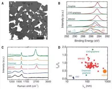
3. Microwave reduction to prepare high quality graphene
(High-quality graphene via microwave reduction of solution-exfoliated graphene oxide)
Efficient stripping of graphite in solution is an ideal way to obtain graphene sheets for printing electronics, catalysts, energy storage and composites. The peeling yield of the lateral large-sized graphite oxide is about 100%, but since the oxygen-containing functional group has not been completely removed, the reduced form of graphene oxide (GO; reduced form: rGO) is still highly disordered. s material. Damien et al. proposed a simple and fast method of reducing GO to pure graphene using a pulsed microwave of 1 to 2 seconds. The excellent structural properties make the microwave-reduced graphene (MW-rGO) exhibit mobility characteristics of more than 1000 cm 2 /V·s when applied to the field effect transistor channel material, and can be used as a highly active catalyst for oxygen evolution reaction. (Science DOI: 10.1126/science.aah3398)

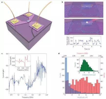
4. Observation and coherent control of interface induced electron resonance in FET
(Observation and coherent control of interface-induced electronic resonances in a field-effect transistor)
In solid-state nanostructures, the electronic defect state at the interface of the material is an important source of noise. Even a trapped charge can qualitatively change the characteristics of short one-dimensional nanowire field effect transistors (FETs) and qubits (qubits) devices. For future nanotechnology, understanding the dynamics of trapping charge is necessary, but direct detection and manipulation is still quite challenging. Tenorio-Pearl et al. transistor-based devices create and detect electronic defect states driven by pulsed microwave coherence. It is noteworthy that their resolution of high-quality resonances in a large number of transistor currents is a function of microwave frequency, demonstrating long regressive coherence time (∼1 μs - 40 μs) and coherent control of defect-induced kinetics. They effectively characterize more than 800 individually addressable resonances through two independent defective host materials, thereby suggesting that their properties are consistent with weakly driven two-stage systems. (Nature Materials DOI: 10.1038/NMAT4754)

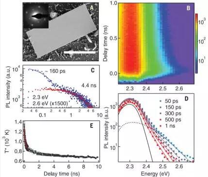
5. Shielding high-energy carriers from crystallization liquids in mixed perovskites
(Screening in crystalline liquids protects energetic carriers in hybrid perovskites)
Despite the existence of static and dynamic disorder, the hybrid lead-halide perovskite exhibits similar carrier characteristics to pure non-polar semiconductors, but it is still unknown how carriers avoid high-efficiency scattering of charged defects and optical phonons. . Zhu et al. revealed this protection mechanism by comparing three single-crystal lead halide perovskites CH3NH3PbBr3, CH(NH2)2PbBr3 and CsPbBr3. They observed the fluorescence of high-energy carriers with a lifetime of about 100 picoseconds in CH3NH3PbBr3, CH(NH2)2PbBr3, but not in CsPbBr3. Thermal fluorescence is associated with reorientation of liquid-like molecules, indicating that at the time scale matched to ultrafast cooling times, dynamic shielding protects high energy carriers by dissolution or formation of large polarons. Similar protection mechanisms may also exist in banded carriers. Long-lived high-energy carriers may be able to make hot-carrier solar cells more efficient than the Shockley-Queisser limit. (Science DOI: 10.1126/science.aaf9570)

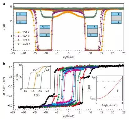
6. Superconducting exchange coupling between ferromagnetics
(Superconducting exchange coupling between ferromagnets)
Recently, discoveries in superconductor (S)/ferromagnetic (FM) heterostructures include: π-junction, triple pairing, critical temperature (Tc) control in FM/S/FM superconducting spin valves (SSVs) Critical current control in the S/FM/N/FM/S spin valve Josephson junction (N: common metal). In these findings, the magnetic state of the device controls the superconducting response, which is usually determined by the applied field. Recently, Zhu et al. reported an observation of the inverse effect, direct superconducting control of the magnetic state in GdN/Nb/GdN SSVs. An antiferromagnetic efficient exchange interaction model based on coupled superconducting condensing energy to a magnetic state can explain the dependence of thickness and temperature on this effect. This superconducting exchange interaction is fundamentally different from the various exchange coupling phenomena caused by conventional spintronics and provides a mechanism for actively controlling the magnetic state in superconducting spintronics. (Nature Materials DOI: 10.1038/NMAT4753)

7. Thermoelectric detection and imaging of graphene plasma propagation
(Thermoelectric detection and imaging of propagating graphene plasmons)
The use of all-electronics to control, detect, and generate propagating plasma is at the heart of integrated chip nano-optics. The graphene carrier long-life plasma is severely limited and controlled by the electrostatic field. However, electronic detection of medium ion propagation of graphene has not been achieved. Mark et al. proposed a full graphene mid-infrared plasma detector operating at room temperature, in which a single graphene sheet acts as both a plasma medium and a detector, rather than by the addition of optoelectronic materials. And it has been successfully implemented in other plasma systems. The device can directly convert the plasma's natural decay product, electron heat, into a voltage through the thermoelectric effect through the thermoelectric effect. Mark et al. added two local gates to adjust the thermoelectric and plasma properties of graphene. High-resolution real-world photocurrent maps can be used to study plasma propagation, interference, decay, thermal diffusion, and thermoelectric generation. (Nature Materials DOI: 10.1038/NMAT4755)

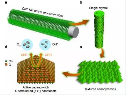
8. Control surface atomic structure to prepare excellent electrocatalyst
(Engineering surface atomic structure of single-crystal cobalt (II) oxide nanorods for superior electrocatalysis)
The surface structure is regulated at the atomic scale to accurately and efficiently manipulate the activity and persistence of the catalyst. Recently, the Australian Qiao Shizhang team reported the regulation of the atomic structure of one-dimensional single crystal CoO nanorods by creating oxygen vacancies on the pyramid surface. These CoO nanorods exhibit excellent catalytic activity and stability against oxygen reduction and oxygen evolution. Experimental and theoretical studies have shown that the origin of the catalytic activity of single crystal CoO nanorods is the oxygen vacancies of the {111} crystal plane. These oxygen vacancies can change the electronic structure of CoO, ensuring rapid electron transfer and optimal adsorption energy. The results of this study indicate that surface atomic structure regulation is an important method for preparing effective and stable electrocatalysts. (Nature Communications DOI:10.1038/ncomms12876)
This article is authorized by the new material online (micro signal: xincailiaozaixian), if other media need to reprint, please contact the new material online small series (micro signal)

Pressure Transmitter

pressure transmitter is a device that converts pressure into a pneumatic signal or an electric signal for control and remote transmission. Pressure Sensor can convert the physical pressure parameters such as gas and liquid felt by the load cell sensor into a standard electrical signal (such as 4~20mADC, etc.), to supply secondary instruments such as indicating alarms, recorders, regulators, etc. for measurement and indication and process regulation.

pressure transmitter

Pressure transmitters are used in various industrial automatic control environments, involving water conservancy and hydropower, railway transportation, intelligent buildings, production automatic control, aerospace, military industry, petrochemical, oil wells, electric power, ships, machine tools, pipelines and many other industries.


There are two types of pressure transmitters: electric and pneumatic. The uniform output signal of the electric type is a direct current signal such as 0-10mA, 4-20mA or 1-5V. The unified output signal of the pneumatic type is the gas pressure of 20-100Pa.

Pressure transmitters can be divided into force (torque) balance type, capacitive type, inductive type, strain type and frequency type according to different conversion principles.

Our advantageous products are mainly compact pressure transmitters, pressure transmitters with display, differential pressure transmitters, wind pressure transmitters, etc.

High Temperature 5

The main advantage

1. The pressure transmitter has the characteristics of reliable operation and stable performance

2. Dedicated V/I integrated circuit, less peripheral components, high reliability, simple and easy maintenance, small size, light weight, and extremely convenient installation and debugging;

3. Aluminum alloy die-casting shell, three-terminal isolation, electrostatic spray protection layer, durable;

4. 4-20mA DC two-wire signal transmission, strong anti-interference ability and long transmission distance;

5. LED, LCD, and pointer three kinds of indicator heads, the on-site reading is very convenient. Can be used to measure viscous, crystalline and corrosive media;

6. High accuracy and high stability. In addition to the imported original sensor that has been corrected by laser, the comprehensive temperature drift and nonlinearity of the whole machine within the operating temperature range are finely compensated.

Pressure Transmitter,Pressure Transducer Sensor,Digital Pressure Sensor,Pressure Transmitter 4-20Ma

Wuxi Winsun Automation Instrument Co., Ltd , https://www.winsunwx.com